Basic Computer Design
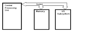
The major components of the computer System are:
- Central Processing unit : It is the brain of the computer system . It is also responsible for deciding the task
- Memory : It is a part of the computer it is responsible for storing the data temporarily and the commands given by the central processor
- I/O systems :This is the piece of the PC that interfaces with the outside world. In the event that a PC didn’t have an I/O framework then it would not be valuable for anything.
- Bus :A bus is a set of common lines, one for each bit of a register, through which binary information is transferred one at a time
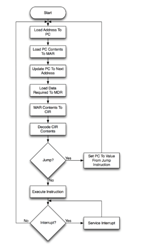
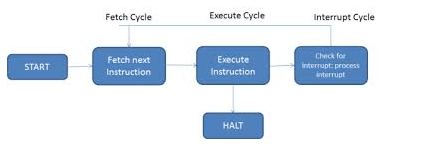
Instruction Cycle
Instruction Cycle :A program dwelling in the memory unit of a PC comprises of a succession of guidelines. These guidelines are executed by the processor by experiencing a cycle for every guidance.A program residing in the computer memory unit of the computer consists of sequence of instructions. In a basic computer each instruction consists of the following phases:
Instruction cycle includes the following phase:
1.Fetch an instruction from memory.
2.Decode the instruction.
3.Read the effective address from memory if the instruction has an indirect address
4.Execute the instruction.
After step 4 the control gets back to step 1 to fetch ,decode and execute the next instruction .
The process continues unless a HALT instruction is encountered.
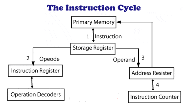
Fetch and decode :
PC is loaded with the address of the first instruction in the program , i.e its stores address of the next instruction
The micro-operation of the Fetch and decode are as follows;
- To:AR<-PC
- Here at intial time t0 the content of PC is transferred to the address register .
- T1:IR<-M[AR],PC<-PC+1
- At time T1 the content of memory pointed by the address register will be transferred to the IR,ie the address of the next register is present in the address register and the instruction located at the address register will be transferred to the instruction register . PC is incremented by one because address is been sent to IR and we need to load the instruction to be executed.
- T2 :Do,,,,,,,,,,,,,,,,D7 <-Decode IR(12-14),AR<-IR(0-11), l<-IR(15)
- At the time T2 instruction will start IR contains instruction which is to be decoded , decoding operation takes place based on the opt Code bits i.e ,Optcode bit of IR 12 -14 will be decoded along with D0 ,,,,,,,,,,,,,,,,,,,D7 line will be enabled . the left over 0-11 bits of IR is Now stored in the address register ,The 15th bit of IR register is meant for direct or indirect memory referencing .
Determining The type of Instruction
During the time T3 the control unit determines the type of instruction i.e, memory reference,Register reference or input-output instruction.
If D7 = 1
Then instruction must be register reference or input-output else memory reference instruction .
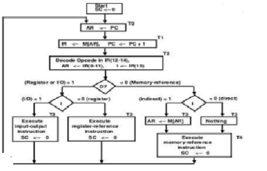
Explanation of the Block Diagram
* Here at initial time T0 the content of PC is transferred to the address register .
* At time T1 the content of memory pointed by the address register will be transferred to the IR.
* Decoding operation begins , IR 15 bit is transferred to 15 bit flipflop .
* The instruction is decided based on T7. If T7 =1 it is ether register or IR, it is decided on the IR 15th bit if Ir =1 ,then it is input out put instruction and makes Sequence counter to be 0
* If I =0 Then it is register executes reference instruction and makes Sequence counter to be 0 .
* If D7 is not equal to 0.Then that means its always going to be memory reference register . There are two types in memory reference instruction it is either direct or indirect it is decided based on the I bit .
* If I =1 then it is indirect addressing that means we have to fetch the effective address , AR<-M[AR] , the address register contains the actual address of the operand then its executes memory reference instruction and makes Sequence counter to be 0 .
*Memory reference instruction is not fixed on timing some my complete at T4 some at T7 depending on that Sequence counter to be 0 .
* If I bit =0 the AR contains direct addressing then memory reference stored in will not be affected there is nothing been carried out at time T3 , After that memory reference counter is executed and Sequence counter to be 0 .
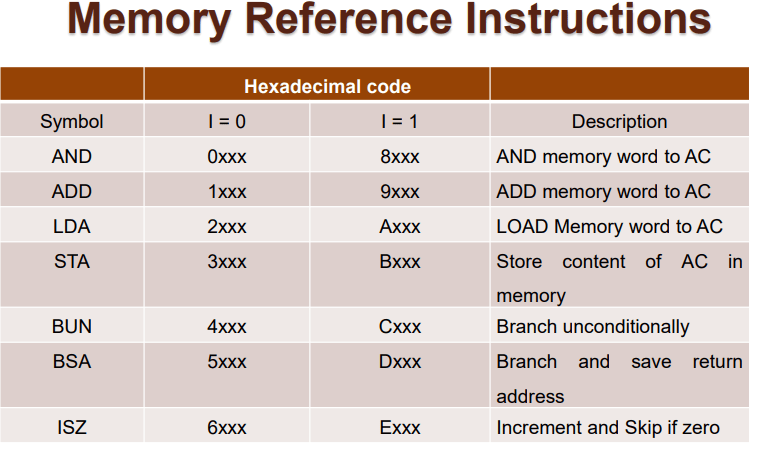
Memory Reference Instruction
In Memory reference instruction .
- First 12 bits(0-11) specify an address.
- Next 3 bits specify operation code (opcode).
- Left most bit specify the addressing mode I I = 0 for direct address I = 1 for indirect address initial 12 bits (0-11) determine a location.
- The location field is signified by three x’s (in hexadecimal documentation) and is identical to 12-piece address.
- The last mode bit of the guidance speaks to by image I.When I = 0, the last four bits of a guidance have a hexadecimal digit identical from 0 to 6 since the last piece is zero
- When I = 1 the last four bits of a guidance have a hexadecimal digit identical from 8 to E since the last piece is one .
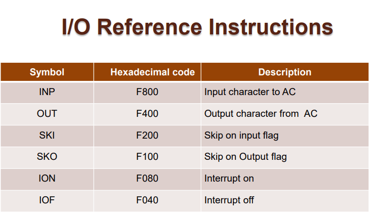
INPUT-OUTPUT INSTRUCTIONS
In I/O Reference Instruction
* First 12 bits (0-11) specify the I/O operation.
* The next three bits equals to 111 specify opcode.
* The last mode bit of the instruction is 1.
* Therefore, left most 4 bits are always 1111 which is equal to hexadecimal F.
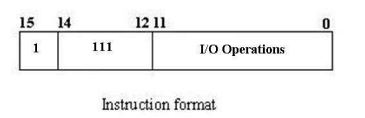
Input/Output – These instructions are for communication between computer and outside environment. The IR(14 – 12) is 111 (differentiates it from memory reference) and IR(15) is 1 (differentiates it from register reference instructions). The rest 12 bits specify I/O operation
- Example –
IR register contains = 1111100000000000, i.e. INP after fetch and decode cycle we find out that it is an input/output instruction for inputing character. Hence, INPUT character from peripheral device.
The set of instructions incorporated in 16 bit IR register are:
- Arithmetic, logical and shift instructions (and, add, complement, circulate left, right, etc)
- To move information to and from memory (store the accumulator, load the accumulator)
- Program control instructions with status conditions (branch, skip)
- Input output instructions (input character, output character)
Interrupt Cycle
An instruction cycle (sometimes called fetch-and-execute cycle, fetch-decode-execute cycle, or FDX) is the basic operation cycle of a computer. It is the process by which a computer retrieves a program instruction from its memory, determines what actions the instruction requires, and carries out those actions. This cycle is repeated continuously by the central processing unit (CPU), from boot upto when the computer is shut down.
Block diagram of Interrupt Cycle
- After the execute cycle is completed, a test is made to determine if an interrupt was enabled (e.g. so that another process can access the CPU)
- If not, instruction cycle returns to the fetch cycle
- If so, the interrupt cycle might performs the following tasks: (simplified…)
- move the current value of PC into MBR
- move the PC-save-address into MAR
- move the interrupt-routine-address into PC
- move the contents of the address in MBR into indicated memory cell
- continue the instruction cycle within the interrupt routine
- after the interrupt routine finishes, the PC-save-address is used to reset the value of PC and program execution can continue